Molecular design for nanolithography: The difference is in the details
Bastienne Wentzel
”For the first time, I feel I am doing research that has an impact. It is very rewarding. I am confident that we are developing materials that can be used in industry.” Sonia Castellanos, group leader of the EUV Photoresists group of ARCNL, unravels the working mechanisms of new classes of photoresists and developes new materials that will make future chips for phones and computers much smaller. Recently, she published results from this research in the Journal of Materials Chemistry C.
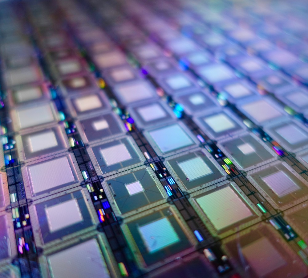
Smaller chips can store more information and make electronic devices faster. But there is a limit to how small a chip can be. The features on these chips must be fabricated using lithography where UV light etches a mask onto the surface. When the features are smaller than 20 nanometer, normal UV light fails and extreme UV light (EUV) becomes the best solution.
Ragged patterns
Problem solved? Not really. EUV light contains a lot more energy than normal UV, which causes problems when it is used to print a pattern in the surface material. This material, called photoresist, absorbs the photons (particles of light) causing chemical changes that reveal the pattern on the chip. Traditionally, polymers are used as photoresists but these do not absorb EUV light very efficiently and they cannot resolve very small features on chips.
Perfect choice
With the disadvantages of polymers in mind and using her background in chemistry, Castellanos thought of another material. ”We need a material that will absorb photons efficiently, enabling us to shorten the exposure time to EUV light. It also needs to be a small molecule so that the features created with light on the chip will be well defined. I chose metal-oxo clusters for this. The metal core of these compounds absorbs the light. The outer shell of organic ligands we can use to modulate the properties of the material such as its solubility and its reactivity.” Castellanos set out to study the way these new materials react to EUV light, and then to chemically modify them to make better photoresists.
“The choice for this material turned out perfectly,” says Castellanos. ”With just one modification, we can significantly change the absorption of EUV light. This means that we can modify the materials to be more or less efficient when printing the optical pattern. They are also much more robust in the high energy conditions that EUV creates.”
Bombarding clusters
Castellanos studied the materials, called metal-oxo clusters, with a method that has not been used before for this type of compound. She went to the SOLEIL synchrotron facility in Paris where the molecules are bombarded with relatively high energy photons, creating ions and fragments that emulate the ionization process that happens with EUV. By using an ultra-high vacuum, the clusters were in the gas phase and the resulting fragments and ions were studied with mass spectrometry. ”This way, we were able to trap the molecules and analyze every individual fragment and ion that was created after the photon bombardment. This is how we established the amount of energy needed to ionize the clusters. In principle, the less energy you need for ionization, the more chemical changes per photon you can expect. This makes the photoresist perform more efficiently.”
”We now have a much better idea of which ligands improve the efficiency of the materials,” says Castellanos. “The main result of this fundamental study is a better knowledge on how to make new photoresist materials that work better in the latest EUV lithography equipment.”
This news article was published as ARCNL Highlights